NVIDIA CEO Jensen Huang had introduced the new NVIDIA H100 Tensor Core GPU at NVIDIA GTC, 2022. The GPU is based on NVIDIA’s new Hopper GPU architecture. Its predecessor, NVIDIA A100, is one of the best GPUs for deep learning. Is H100 a better successor? How do they compare? Analytics India Magazine analyses this.
Difference Between H100 Vs A100
| Feature | NVIDIA H100 | NVIDIA A100 |
|---|---|---|
| Architecture | Hopper | Ampere |
| Process Technology | 4 nm | 7 nm |
| CUDA Cores | 16,896 | 6,912 |
| Tensor Cores | 528 | 432 |
| Memory | 80 GB HBM3 | 40/80 GB HBM2e |
| Memory Bandwidth | 3.35 TB/s | 2.0 TB/s |
| Peak FP64 Performance | 60 TFLOPS | 9.7 TFLOPS |
| Peak FP32 Performance | 60 TFLOPS | 19.5 TFLOPS |
| Peak FP16 Performance | 1,000 TFLOPS | 312 TFLOPS |
| NVLink Bandwidth | 900 GB/s | 600 GB/s |
| PCIe Generation | PCIe Gen 5 | PCIe Gen 4 |
| TDP (Thermal Design Power) | 700W | 400W |
| Target Applications | AI, HPC, Data Analytics | AI, HPC, Data Analytics |
The H100
The NVIDIA H100 is the company’s ninth-generation data centre GPU packed with 80 billion transistors. Based on the Hopper architecture, NVIDIA claims it to be “the world’s largest and most powerful accelerator”, perfect for large-scale AI and HPC models. This is given the GPU’s features like:
- World’s Most Advanced Chip
- New Transformer Engine that speeds up networks 6x the previous version
- Confidential Computing
- 2nd-Generation Secure Multi-Instance GPU with MIG capabilities extended by 7x the previous version
- 4th-Generation NVIDIA NVLink connecting up to 256 H100 GPUs at 9x higher bandwidth
- New DPX Instructions that can accelerate dynamic programming by up to 40x compared with CPUs and up to 7x compared with previous-generation GPUs.
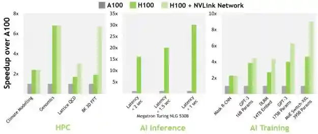
NVIDIA promises the new GPU and Hopper technology will power the most upcoming research in AI. This is given the highly scalable NVLink® interconnect for advancing gigantic AI language models, deep recommender systems, genomics and complex digital twins. Additionally, it allows for enhanced AI inference supporting real-time and immersive applications using giant-scale AI models, chatbots with the capacity for real-time conversation based on Megatron 530B, the most powerful monolithic transformer language model and training of massive models with a speedier process.
NVIDIA A100
NVIDIA A100 Tensor Core GPU, announced in 2020, was then the world’s highest-performing elastic data centre for AI, data analytics, and HPC. The Ampere architecture provides up to 20X higher performance than its predecessor, with the ability to divide into seven GPUs and dynamically adjust to shifting demands. Supporting the huge digital transformation wave in 2020 and the pandemic, A100 GPU features a multi-instance GPU (MIG) virtualisation and GPU partitioning capability, efficient for cloud service providers (CSPs). Amidst MIG, the A100 allows CSPs improvement to deliver up to 7x more GPU Instances. In addition, the GPU includes the new third-generation Tensor Core that boosts throughput over V100 and supports DL and HPC data types.
Architectural Difference Between H100 Vs A100
NVIDIA Hopper
The NVIDIA Hopper, named after scientist Grace Hopper, was released two years after the previous NVIDIA Ampere architecture. The Hopper architecture extends MIG capabilities by up to 7x over the previous generation by offering secure multitenant configurations in cloud environments across each GPU instance. It introduces features to improve asynchronous execution and allow an overlap of memory copies with computation while minimising synchronisation points. Hopper also mitigates the issues of long training periods for giant models while maintaining the performance of GPUs. The architecture is created to accelerate the training of Transformer models on H100 GPUs by 6x.
NVIDIA Ampere
NVIDIA’s Ampere architecture has been described as the “heart of the world’s highest-performing, elastic data centres.” Ampere supports elastic computing with high acceleration at every scale. The architecture is crafted with 54 billion transistors, making it the largest 7 nanometers (nm) chip ever built. In addition, it provides L2 cache residency controls to manage data to keep or evict from the cache, further supporting the growth of data centres. Ampere consists of NVIDIAs’ third generation of NVLink®, allowing it to scale applications across multiple GPUs with doubled GPU-to-GPU direct bandwidth to 600 gigabytes per second (GB/s).
Specification Difference Between A100 Vs H100
| Features | NVIDIA A100 | NVIDIA H100 |
| Transistors | 54.2 Billion | 80 Billion |
| GPU DIE Size | 826 MM2 | 814 MM2 |
| TSMC Process | 7NM N7 | 4N |
| GPU Architecture | NVIDIA Ampere | NVIDIA Hopper |
| Compute Capability | 8.0 | 9.0 |
NVIDIA H100
NVIDIA’s H100 is fabricated on TSMC’s 4N process with 80 billion transistors and 395 billion parameters, offering up to 9x faster speed than the A100. “NVIDIA H100 is the first truly asynchronous GPU”, the team stated. The GPU extends A100’s ‘global-to-shared asynchronous transfers’ across the address spaces. It also grows the CUDA thread group hierarchy with a new level called the thread block cluster.
The H100 builds upon the A100 Tensor Core GPU SM architecture, enhancing the SM quadrupling the A100 peak per SM floating-point computational power and 0.0 compute capacity. This is given the FP8, doubling A100’s raw SM computational power on all previous Tensor Core, FP32, and FP64 data types, clock-for-clock. As listed by NVIDIA, these are the general specifications of H100.
- 8 GPCs, 72 TPCs (9 TPCs/GPC), 2 SMs/TPC, 144 SMs per full GPU
- 128 FP32 CUDA Cores per SM, 18432 FP32 CUDA Cores per full GPU
- 4 Fourth-Generation Tensor Cores per SM, 576 per full GPU
- 6 HBM3 or HBM2e stacks, 12 512-bit Memory Controllers
- 60MB L2 Cache
- Fourth-Generation NVLink and PCIe Gen 5
NVIDIA A100
The A100 is built upon the A100 Tensor Core GPU SM architecture, and the third-generation NVIDIA high-speed NVLink interconnect. The chip consists of 54 billion transistors and can execute five petaflops of performance; a 20x leap from its predecessor, Volta. In addition, with a computing capacity of 8.0, the A100 includes fine-grained structured sparsity to double the compute throughput for deep neural networks. As listed by NVIDIA, these are the general specifications of A100.
- 8 GPCs, 8 TPCs/GPC, 2 SMs/TPC, 16 SMs/GPC, 128 SMs per full GPU
- 64 FP32 CUDA Cores/SM, 8192 FP32 CUDA Cores per full GPU
- 4 third-generation Tensor Cores/SM, 512 third-generation Tensor Cores per full GPU
- 6 HBM2 stacks, 12 512-bit memory controllers
Conclusion
The NVIDIA H100, based on the Hopper architecture, represents a significant leap over the A100, which is based on the Ampere architecture. The H100 features a more advanced 4 nm process technology, significantly more CUDA and Tensor Cores, and higher memory bandwidth with HBM3 memory. It also offers superior performance across various precision levels (FP64, FP32, FP16) and enhanced NVLink bandwidth, making it a powerhouse for AI, HPC, and data analytics applications. The A100, while still highly capable, is built on a 7 nm process and offers robust performance suitable for similar applications but with lower overall specifications compared to the H100.


